What actually is a PCB redesign? Now is the time!
One of the services that we commonly do in ASN Plus for our customers is the PCB redesign. Companies request the reworking of existing electronics designs from our company more and more often. They need to update it to match their actual demands.
We have decided to sum up the most important information which is related to the redesign.
What is the PCB redesign
First, it is important to realize that the redesign is not just a simple redrawing the PCB to the new form. It is mainly a complex process which consists of a series of consecutive steps. It includes precision verification of existing manufacturing documentation, then its transformation to the new development interface or checking all of the components. It cannot be done without careful update of both, schematics and layout and subsequent verification of the new design.
The most common reasons for PCB redesign
What are the reasons for redesign? There are plenty of them, the most frequent are the following two: lack of the components and general improvement of an existing device.
The lack of electronic components
The interest in PCB redesign due to lack of electronic components was quite huge during the last month. Some of the producers were forced to limit or even stop their production due to the recent pandemic. It resulted in lack of components or in significant price increase. „In recent months, redesign due to lack of the components is in our company one of the most required services.” confirms our CEO Pavel Schiller.
The component might be unavailable even for a more prosaic reason - it's the end of its production. The components are not at the end of the life cycle (EOL) suitable for another production and are signed as „Not recommended for a new design”. In this case it is necessary to process a redesign well in advance and to find suitable alternatives, which might bring even more benefits due to general technological progress.
Innovation of the existing product
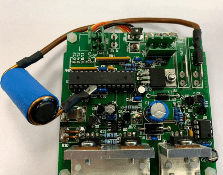
The second most frequent reason for redesign is the improvement of existing solution or adding the functionalities. „In the past, we have been processing product innovation for an example during the golf wagon control unit redesign for company Elmet.” adds Pavel Schiller. „In this particular case it was necessary to completely rework unit electronics including its firmware. We have managed to reduce the manufacturing costs at the same time.”
When is the right time for electronics redesign?
There might be at least two scenarios for the electronics redesign: the product innovation or lack of components. If the goal of the redesign is electronic device modernisation, there is enough time for the preparation. The opposite situation, and much worse, is when the redesign has to be processed due to the lack of components.
The request comes usually at a moment when the factory learns that there will be mounted PCBs outage, which are necessary for its products. If there is a supply outage, for the company it means a stop of the production, which leads to significant financial losses. Every company wants to avoid cases such as this.
That’s why we rely on reliability and flexibility in ASN Plus. We are prepared for unexpected situations and therefore we are able to react flexibly and solve the problem as soon as possible. The need for PCB redesign can be often detected in advance and thanks to that the company can prepare for the whole process. The critical milestone for the redesign is usually five years since prototype development. After this time it is recommended to do a regular inspection of the components availability. If you are planning the production of a product with only one type without any updates, entrust the production to a company, which has experiences with long term production of mounted PCBs and knows well the components life cycles.
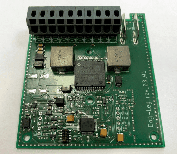
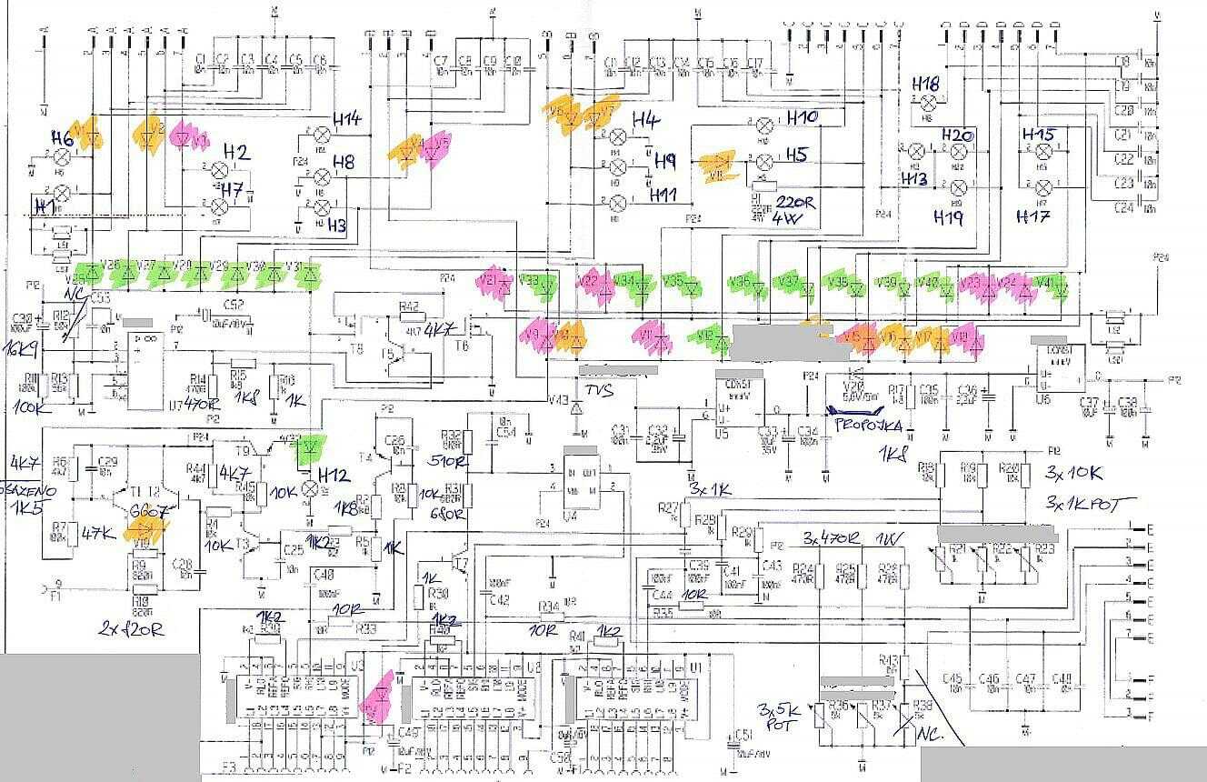
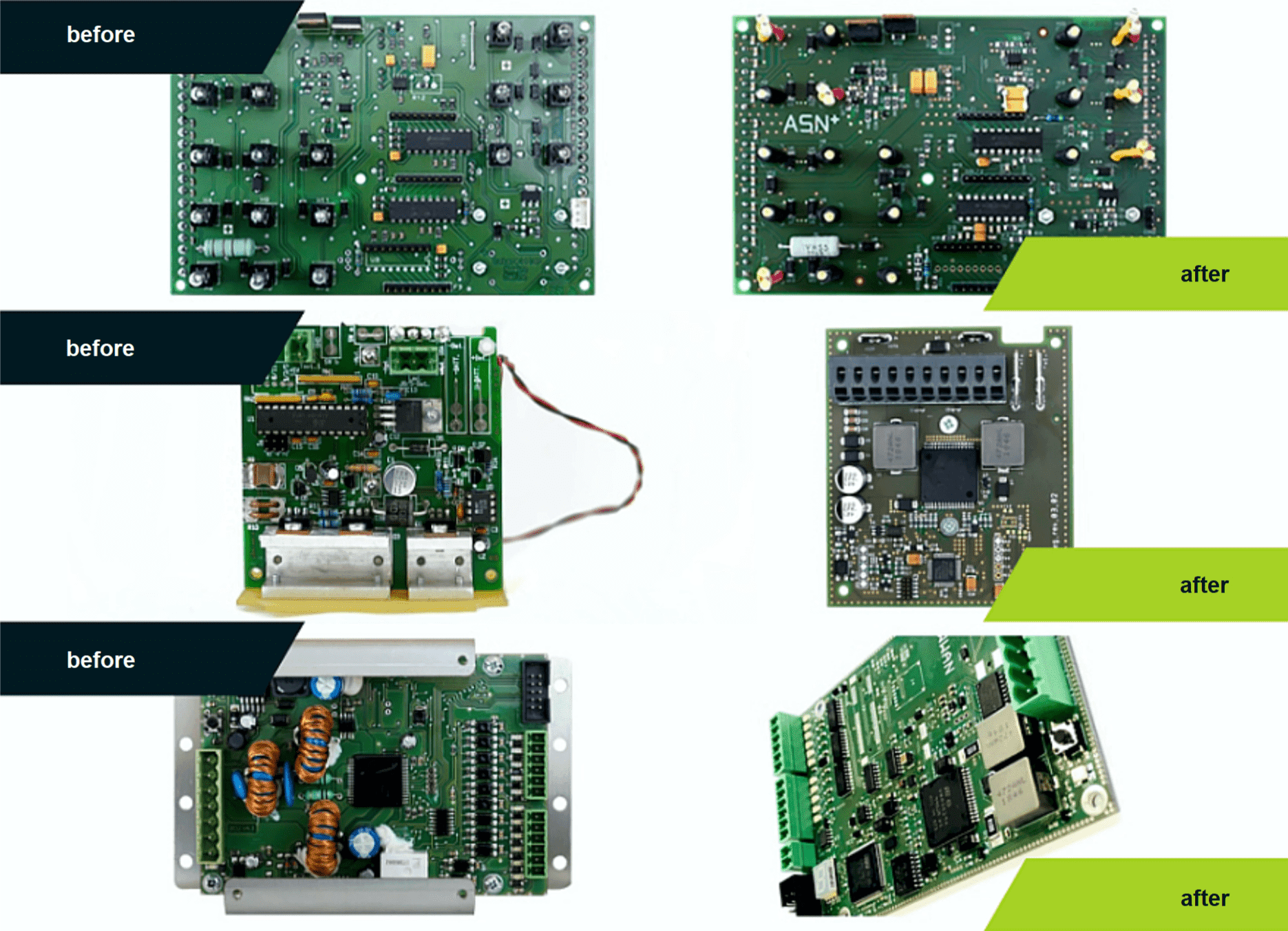
Original PCB before redesign
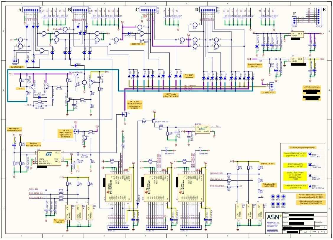
New PCB after redesign
Our tip!
Keep in mind the future redesign when developing the prototype
In case you are still in stage of development of the new electronic device, don’t forget about the probable need for future PCB redesign. If you count on this beforehand, you can save a lot of time and money.
There are important both, practical experiences and suitable development tools during the development that takes into account the future redesign. We work with the professional tool Altium Designer in ASN Plus, which makes future PCB updates easier in a fundamental way.
It included a big amount of assisting functions such as ActiveBOM. Thanks to it, users can easily map components' price and availability among various internet distributors. Another advantage of Altium Designer is its cross-version compatibility. Thanks to it, the user can be sure that he will be able to open and update the PCBs created even five years ago in a new version of Altium Designer. The user does not have to do any advanced transformations and partial updates which makes the redesign even less time consuming.
Paper schematics are no problem for us
If you come to us with existing PCB documentation in electronic form (ideally in Altium Designer), the redesign will be for us a piece of cake. But we are ready for bigger challenges as well! From time to time a customer comes to us with an old box of papers with drawings which are barely readable or with one piece of broken device. We like even projects such as this, our developers approach them with enthusiasm. In these cases, they remember the beginnings of their developers career and use their knowledge of reverse engineering.