About us > ASN News
The evolution of printed circuit boards: driving innovation in electronics
From smartphones to home devices, printed circuit boards (PCBs) are at the heart of electronics today. With increasing demands for faster, smaller and more advanced electronics, PCB technology has evolved dramatically over the past decades through remarkable manufacturing innovations.
In this article, we explore key milestones in PCB manufacturing that have shaped electronics as we know it. We'll look at how PCBs work, trace the history of PCB manufacturing, understand recent advances, and explore the impact of PCBs across industries driving innovation.
How do PCBs work?
Before we get into manufacturing development, let's quickly clarify what PCBs are and how they work.
PCBs are thin boards made of insulating materials, such as fiberglass, with engraved or printed copper traces on the surface. Electronic components such as integrated circuits, resistors, capacitors are soldered and connected to these copper traces called conductors.
When electric current flows through these conductors, it allows the various components to communicate with each other and perform the desired functions. PCBs provide a platform for assembling components and interconnecting them as the cornerstone of any electronic device.
With miniaturization as a major focus, PCBs have continuously evolved from simple single-layer boards to complex multilayer boards enabling high-density component assembly.
Now that we know what PCBs are, let's take a look at the incredible innovations in PCB manufacturing over the decades that have driven the evolution of electronics.
History of innovation in PCB manufacturing
Although the origins of PCBs can be traced back to the 1950s, significant advances in manufacturing technology have shaped the PCB industry and driven innovation in electronics.
1900 - Bakelite boards
-
The earliest PCBs appeared in the early 20th century and were made from materials such as Bakelite and paper phenolic resin. These single-sided, low reliability boards were used in simple radios and amplifiers. Production was also manual and labour intensive.
1950 - Automated production
-
In the 1950s, the electronics industry began to move toward automation using printed circuit technology for commercial applications. Machines for etching copper and drilling holes were introduced, which improved PCB reliability.
1960s - Multilayer PCB
-
With limited space for component mounting, PCBs evolved into a multilayer configuration in the 1960s, allowing components to be placed on either side. Multiple layers of copper were bonded together using insulating material, achieving denser designs.
1970s - Surface mount technology
-
Engineers achieved further space optimization in the 1970s with surface mount technology. Instead of drilling holes for wiring, components were directly soldered to the surface, eliminating the need for drilling.
1980 - The advent of CAD tools
-
Manual PCB layout design failed to keep pace with increasing complexity. The introduction of computer-aided design (CAD) tools revolutionized PCB design, allowing complex PCBs to be designed more quickly and converted to production.
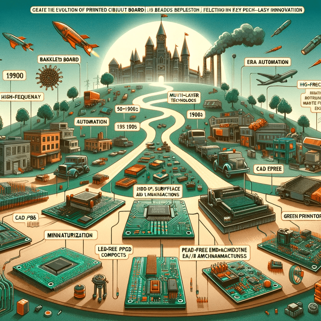
1990 - Dense Packaging
-
Surface mount technology along with CAD tools further spurred miniaturization in the 1990s producing smaller components. PCBs became denser and packaged several small components, becoming a common part of virtually every electronic device.
2000 - Flexible PCBs
-
While traditionally fiberglass was used for the PCB substrate, the 2000s brought the rise of flexible PCBs made from polymer films. Flexible PCBs opened the door to new formats such as wearable devices. Rigid-flexible PCBs also emerged, allowing flexibility only in desired areas.
This incredible innovation in PCB manufacturing during the 20th century forms the basis for the modern electronics industry. But advances are continuing rapidly into the 21st century as demand for sophisticated electronics in industries intensifies.
Recent advances driving PCB innovation
Several new technologies in PCB manufacturing promise to accelerate innovation in electronics and connected devices across sectors in the coming decade.
Let's take a look at some of these key advances shaping the PCB industry:
High frequency materials
-
For high frequency applications such as 5G, WiFi 6 and mmWave devices, conventional PCB materials severely limit electrical performance. Specialized PCB materials designed with high frequency laminates reduce dielectric loss. This enables faster signal transmission, which is crucial for high frequency applications.
3D printing
-
Highly futuristic 3D printing technology is entering PCB prototyping, allowing for greater design flexibility. By printing conductive and insulating materials layer by layer, complex three-dimensional PCB structures can be produced on demand without the cost of tooling.
Microvias in HDI PCBs
-
To produce the complex and compact high-density interconnect (HDI) PCBs needed in smartphones and wearable devices, microvia help connect multiple layers through small holes. Stacking thin layers with laser-drilled microvia meets the requirement for lightweight and reliable mobile devices.
Built-in passive/active elements
-
Traditionally, PCBs and components have been assembled together. But new techniques allow passive elements, such as resistors and capacitors, to be built into the PCB substrate, reducing space requirements. Future PCBs will embed complete ICs, greatly improving electrical performance due to shorter leads.

Lead-free and green production
-
With the rapidly growing need for environmental responsibility for sustainable manufacturing, new lead-free soldering techniques are emerging. Recyclable PCB materials such as biodegradable resin also reduce the waste footprint.
Advanced testing
-
Maintaining quality requires thorough testing to detect defects early. Testing methods such as X-ray diagnostics, in-circuit testing (ICT) and boundary scan testing are becoming more advanced and more thoroughly inspect PCBs before deployment.
AI and ML applications
-
The complexity of PCB design is increasingly benefiting from AI and machine learning driving automation. Wire length optimization, predictive system maintenance, and defect analysis are some areas where AI is finding new applications.
Industry sectors driven by PCB innovation
Relentless innovation in PCB manufacturing is having a profound impact on devices and systems across strategic industries such as consumer electronics, communications, automotive, healthcare and aerospace that depend on electronics.
Here are some examples of PCB advances that are transforming these industries:
Consumer electronics
-
Flexible PCBs in flexible smartphones
-
HDI PCBs packing dense functionality in wearable devices
-
Higher bandwidth PCB materials in WiFi routers
Communications
-
Low-loss PCB materials for 5G NR
-
HDI PCBs in network infrastructure
-
Temperature control with heavy copper PCBs
Automobile industry
-
Automobile PCBs resist vibration, shock
-
Flexibility of PCBs in electronics downsizing
-
Short distance signal transmission for ADAS systems
Aerospace and defence
-
Rigid-flexible PCB withstands extreme temperature fluctuations
-
PCB inspection ensures zero defects in navigation
-
Durable boards withstand mechanical stress
Across sectors, advances in PCBs are at the core of technological innovation, enabling increased functionality, reliability and connectivity in electronic devices.
As artificial intelligence, the Internet of Things, Industry 4.0 and other next-generation technologies continue to rapidly evolve in the coming decade, they will critically depend on parallel innovations in PCB manufacturing to unlock their true potential.

The future of PCB
PCB manufacturing has come a long way, evolving dramatically from manual wiring to automated, AI-driven technologies promising extreme precision and improved performance.
With electronics becoming ubiquitous across applications, PCBs will continue to push the boundaries to include new materials like graphene, new design techniques like interactive 3D modeling, and new manufacturing methods like inkjet printing, all focused on the relentless search for faster, smaller, smarter systems.
As an integral but often overlooked foundation, advances in PCBs will catalyze technological innovation across strategic sectors and drive the future of electronics in the coming decade and beyond.
Become one of our trusted clients


Take your product to the next level!
Book a consultation with our specialists and discover just how many technological possibilities are within your reach. We’ll be in touch soon to explore the best way to work together.
