The most common mistakes in PCB design
In the recent article we focused on the most common mistakes in schematic design. Precisely made schematic is thereby essential for PCB design. Schematic itself is definitely not enough. Let’s move a step further - we will advise you how to design functional PCB on first try without the mistakes.
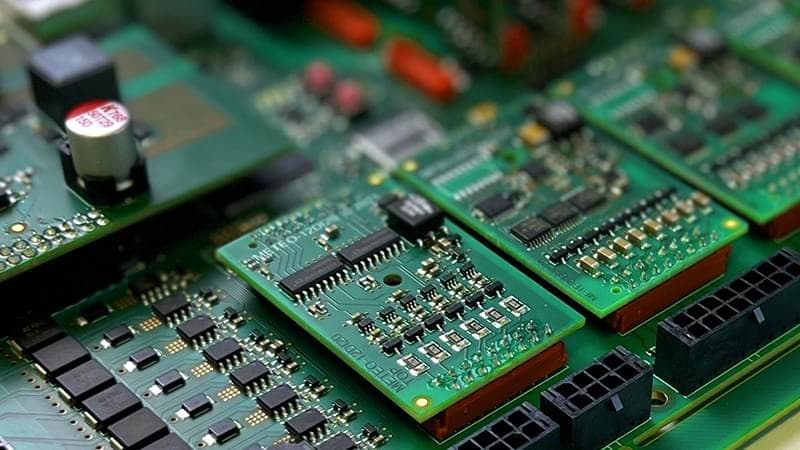
Mistakes in creating footprints
PCB design starts with creating and checking the components in library (footprints). There are tools which will make your preparations easier, so you won’t have to draw it completely from scratch. In our company, ASN Plus, we work with professional software Altium Designer, which contains a feature PCB Component Wizard. It can generate most of the footprints including 3D model. The developer thus does not have to deal with layers, lines width and other technological issues. He just processes component check.
What to focus on when checking the component
It is necessary to process a check of generated footprints. So what are the things to focus on?
Case names
First thing to check is exact case title. Beware of various confusions, such as TSSOP with TQFP, or SOIC Narrow with SOIC Wide. Compare the sizes with data from the datasheet and check components pitch correctness.
„Mirror mistake“
,,Mirror mistake” might occur during creating the footprints without using PCB Components Wizard or other similar tool. It’s concept is mirror footprint turn, which disables correct component assembly.
Incorrect polarity
Component’s case incorrect turn occurs regularly when the signs in assembly drawing is ambiguite. The reason can be a direct manufacturing mistake, when assembly does not correspond with assembly drawing.
That’s why we recommend to deliver also 3D PCB view, or document in *.3dpdf format to the manufacturer. We generate these files thanks to Altium Designer automatically in ASN+. Thus we minimize the risk of mistakes done during assembly and we prevent potential financial losses of our clients.
Correct components placement
It is important to find the right balance between mechanical, electrical and thermal aspects of a PCB. Thermal aspects, or thermal conditions are often forgotten when placing the components during development. It is necessary to secure performance components to be well cooled. It is also important to support the head distribution, whether by using air flow, using cuprum on PCB or placing the coolers.
Sizes and shape of PCB and connector positions or assembly holes are usually part of a task documentation. Paper models are not practically used these days for checking the components placement. More effective way is to use PCBA export models directly to the programme as Autocad. It also offers the option of importing mechanical models to the software for PCB design. You can start designing the PCB from the electrical side after the required board shape and connectors, or integrated circuits are finished.
Electromagnetic compatiblity and system failures
Take into account PCB layout when designing the PCB. Respect correct isolation distances (celarance and creepage) and place selected components according to the voltage level of the signals. It is necessary not only because of correct function, but even because of safety. You will not go through without professional knowledge.
Minimize loop length and frequency spectrum, filter the power supply and use suitable blocking capacitors.
Keep in mind not only horizontal, but also vertical circuit board structure. Focus on stack-up in multi-layered boards, which indicates exact description of all layers including used through holes. Do not forget, that stack-up has influence even on differential pairs impedantion. We recommend to design multilayer PCBs based on manufacturer's offer and thus conduct parametres count yourself (manually, or in development environment).
Development environment and design rules
No matter which development environment you use, set the ,,release procedure” everytime. Use as much as you can the ,,design rules” and related automatic checking service DRC(Design Rule Check), which warns of errors itself. Don’t forget about silkscreen in other words the first layer, which helps to differ particular parts, testing points and warning symbols. Use silkscreen for example to sign the signal names on the connectors.
Open-source projects as a rich source of inspiration
Carry on improving yourself and do not panic, you will get more and more experienced. If you want to get more advanced in PCB design, watch more experienced workers. There are a lot of available open-source projects to analyze and critically evaluate.
For efficient PCB design is important right choice of development environment and it’s perfect knowledge. We have chosen Altium Designer and we can recommend this professional tool to others. We have some tips on sources, where you can find open-source projects for Altium Designer available for download. It can serve as a source of inspiration for beginners and even for advanced developers.
Projects made in Altium Designer are available for download here: