The most common mistakes during schematic design
Are you interested in schematic design? Then take attention for common mistakes which lead to malfunctioning designed electronics. Our engineers have designed that amount of schematics, which could cover the football game field. Thanks to their extensive experience, they know what to avoid. We have decided to sum up their recommendations and pass on the know-how we have been building for years. We believe our tips can help beginners, as well as advanced hardware developers.
Avoid swapping the data wires
One of the basic mistakes which are made during designing the schematic is data line swapping. Typical is swapping signals such as Rx and Tx, SDA, SCL or MISO and MOSI. We have also encountered the wire swapping in buses, which use differential pairs (such as R485 and USB) .
It is important then to focus on checking data wires. We recommend placing 0R resistors on these signals at the same time. In case of need you shall simply cross the signals in the place of resistors.
Focus on clarity and readability
Design your schematics so they are as clear and readable as possible. It is important especially during noting the electronic components value. Do not use note such as 2.2 uF, but 2u2 when noting the condenser. Keep evidence of all components in the schematic, which are contained in the PCB. You will prevent forgetting important components during the production. There should not be missing counterparts of PCB connectors, labels, jumpers and even fasteners in the design.
The purchasing dpt. will thank you for correct marking
Pay attention to component marking during library creation. Inaccurate marking prolongs production and might lead to buying of insufficient components (for example it might look the same but has different parameters). Differentiate what is important in the mark and what is not. For example, only some letters at the end of component names are important for identification. Component part-number has to be accurate without any doubt.
In case of primary component non-availability on the market we recommend to add as many potential component alternatives in the library. The purchasing department will be grateful if you respect the hints mentioned above.
Structure, corporate standards and other factors
PCB Project, of which part is schematic, has to have suitable structure (hieratic, flat, or its variations). It has to work with adequate tools for mutual signal connection(port, power port, harness etc.) at the same time. Use all options for the schematic design which is provided by the development environment. Anyway, the design software will highlight plenty of mistakes itself automatically. We use Altium Designer in our company, which does a fantastic job in this aspect.
Schematic symbol designing
It is important for schematic symbols to be clear and identical with symbols contained in datasheets. For example, the number of pins and their positions must fit. Keep in mind the rule: ,,Make double check of your circuit, triple check of new library parts.” Checking the new library elements must be done even more consistently than checking the schematic itself.
Notes, calculations and specifications
Schematic cover page must contain all things required by corporate standards. On top of that it should also include a series of additional information which will help it’s clarification and make other colleagues work easier. Add your notes from simulations, tabs, calculations, pictures, even concrete tips for layout design into the schematic. You can increase clarity by coloring often used signals as well.
Minimize sticky joints
Crossing lines decrease schematic clarity. Sometimes it is barely recognize on a first sight which lines are connected and which not. Design the schematic to contain only the necessary minimum of crossing lines.
Keep in mind electronics revival, testing and edits
Take into account the future revival, testing and edits of finalized PCB even during designing the schematics. Use resistors, capacitors or ferrite beads. Work with variety of assembly variants - redundant positions leave empty. If you keep enough empty positions, you can use them for future modifications, testing or debugging during EMC testing.
Confusing of clear schematic - example
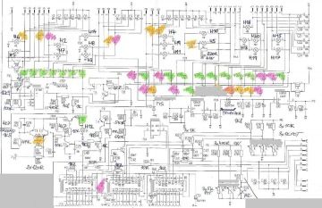
You can see schematic below which is decades old. It does not contain any notes, is barely readable, confusing and full of crossing lines. We have added the notes and colored signs during the PCB redesign.

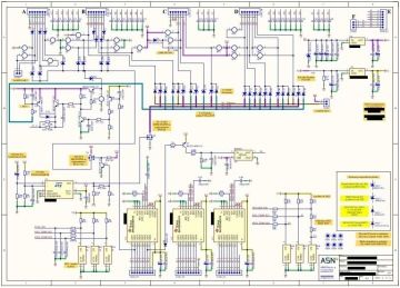
There is schematic after complete rework on the second picture. To keep option of reverse checking, we kept the concept of one schematic cover page. It’s part is colored marking of important signals and many notes, which will make working with schematic easier.

Altium Designer is able to transfer signals coloring on the PCB. It is possible to perform electronics service even without a PC in various demanding environments thanks to this feature. It is also worth mentioning the software background of Altium Designer - fast access to datasheets and 3D models or BOM generating. The original document would not enable this feature without any doubt.
We recommend to every company to sum up all design mistakes and create a checklist. It should be with additional checking mechanisms a part of the release procedure.
When your schematic is clear and precisely checked, you can go on to the PCB design. But even in this part there is a lot of traps for developers. That’s why the most common mistakes during the PCB design is a topic of our next article.